
The serial architecture processes one symbol per clock cycle, whereas that the parallel architecture processes four symbols per clock cycle; each symbol is represented only by two samples. The communication system is assume to have stable emission clock and a receiver clock with a precision of 5 ppm (standard deviation of the variation of the number of clock cycles per million) and 50 ppm, with the clock frequency of the receiver slightly higher than the clock frequency of the transceiver.
The BER curve is presented to show the performance of these architectures with fixed point simulation in MATLAB. The VHDL code of these architectures is simulated with ModelSim with the same input source as in MATLAB.
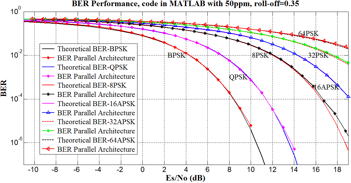
The designed architecture has been implemented with a Xilinx XC6VLX240T-1FF1156 FPGA chip, and reaches the maximum running frequency of 280 MHz. Thus, the architecture sustains a symbol rate of 1.12 G symbol/s (i.e. from 1.12 Gbit/s for BPSK up to 6.72 Gbit/s when 64 APSK signal is used). Performance are characterized for several roll-off of the Nyquist filter: 0.01 up to 0.35. As an illustration, Fig. 1 compare the Bit Error Performance (BER) as a function of $E_s/N_0$ between theory and actual design. In this figure, the receiver clock is supposed to be 50 ppm (part per million) faster than the transmission clock.
Figure 1: BER performance of the proposed algorithm.
As can be seen in this figure, the proposed algorithm reach almost optimal performance for a very large range of $E_s/N_0$ (from -10 dB to 15 dB), and for several constellation (BPSK up to 64 APSK).
This work has been done between INICTEL-UNI and the Lab-STICC. Hardware used in this project has been funded by the project PALMYRE II (Brittany region and FEDER funding).
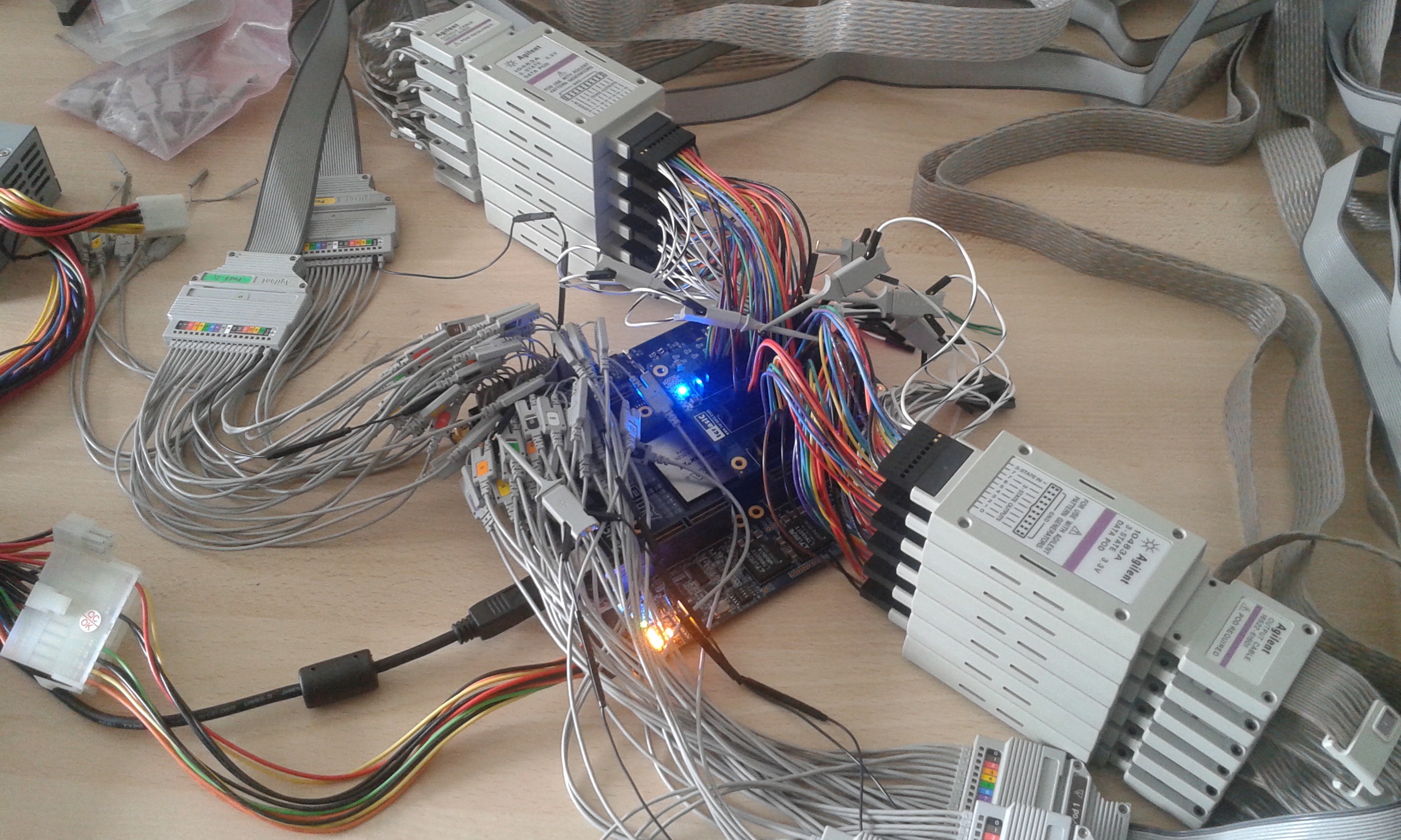
Figure 2: FPGA Board with connectors.
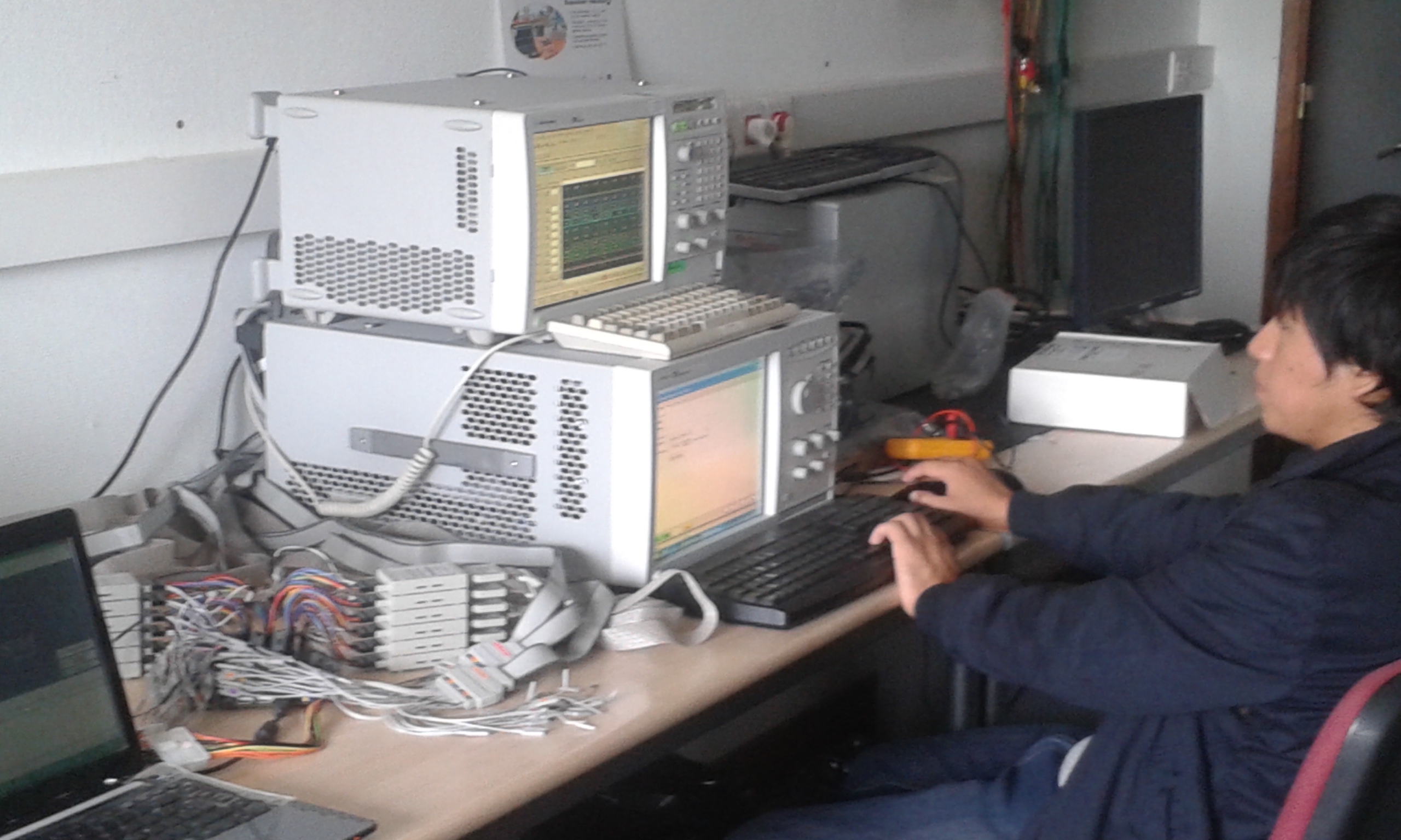
Figure 3: Whole hardware test system.
Return to main page of Emmanuel Boutillon